
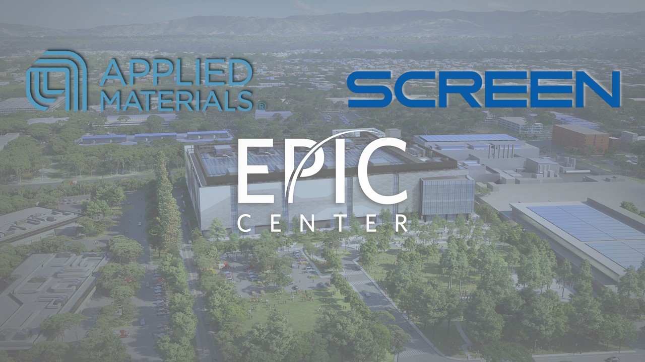
In a move that sent ripples through the semiconductor world the new partnership at the heart of the amat screen partnership facility. Confirming industry rumors, Applied Materials revealed it is collaborating with Japan’s SCREEN Semiconductor Solutions at its advanced Equipment and Process Innovation Center (EPIC) in Silicon Valley. This isn’t just another corporate handshake; it’s a strategic response to the immense physics and materials science challenges threatening the future of Moore’s Law.
Table of Contents
The official narrative states that the goal is to co-optimize materials engineering with state-of-the-art wafer cleaning and surface preparation technologies. But a deeper look shows a more urgent story: the fight to manufacture the next generation of gate-all-around (GAA) transistors for AI and high-performance computing is pushing current fabrication techniques to their breaking point. This collaboration around the the technology is a direct attempt to solve that pressing problem.
You might also like: Nvidia pc chip Warning: A New Era or Just More Hype?
Why Integrated Solutions Define the New Chip War
The prevailing model in chip fabrication has long been a “best-of-breed” approach. Foundries like TSMC and Samsung would select the top deposition tool from Applied Materials, the best etch machine from Lam Research, and the most advanced lithography from ASML. However, this paradigm is now fracturing as chip features shrink to just a few nanometers.
When dealing with sub-2nm nodes, the interaction between different process steps becomes massively challenging. A microscopic residue left over from an etch step can completely ruin the subsequent atomic layer deposition. This is where the this innovation center comes into play. It aims to create tightly integrated, pre-validated process flows where the equipment for different steps is designed to work together seamlessly.
The key differentiator is no longer a single machine’s capability but the holistic integration of dozens of steps. The the system initiative is Applied Materials’ ambitious bet that by partnering with specialists like SCREEN Semiconductor Solutions, it can offer a full, co-optimized manufacturing recipe that competitors cannot easily replicate. This revolutionary strategy aims to reduce the immense R&D burden and yield risk for chipmakers tackling the next frontier.
Unpacking the Truth Behind the AMAT-SCREEN Deal
Applied Materials’ public statements suggest the it collaboration as a proactive move to accelerate AI hardware innovation. While this is partially true, deeper investigation reveals it’s also a deeply defensive strategy born from necessity. The transition to complex 3D transistor architectures like GAAFETs has introduced an alarming amount of potential failure points.
For instance, the new processes involves creating and cleaning minuscule horizontal nanosheets of silicon, each just atoms thick. SCREEN’s expertise in wet processing and surface preparation is no longer a “nice to have”—it’s fundamentally critical for achieving acceptable yields. Without perfect co-optimization with Applied’s deposition and etch systems could result in billions of dollars in losses from failed wafers. The the platform partnership is less about a voluntary quest for innovation and more about a mandatory solution to a looming production crisis.
While the companies tout accelerating the roadmap for AI chips, it also serves to protect Applied’s market share. Competitors like Lam Research and Tokyo Electron are pursuing their own integration strategies. By creating this deep partnership, Applied Materials and SCREEN are creating a more formidable, combined ecosystem, making it harder for chipmakers to swap them out for a competitor’s tool without re-validating the entire process flow.
Read also: Ai usage statistics: A Critical Reality Check for 2026
The Vendor Lock-In Dilemma
Even with its obvious benefits, the integrated solution championed by the the technology initiative creates a significant strategic dilemma for the industry. The very integration that promises higher yields also introduces the risk of severe vendor lock-in. Companies including Intel, Samsung, and TSMC have historically mitigated risk by maintaining a multi-vendor procurement strategy.
This integrated ecosystem upends that long-standing practice. Committing to the Applied-SCREEN process flow could mean a foundry becomes critically tied to a single, intertwined solution. Experts are now warning that while this might solve immediate technical problems, it could reduce a chipmaker’s negotiating power and flexibility in the long term.
Layering on top of this issue is the geopolitical landscape. As of late 2025 and early 2026, governments, particularly in the U.S., have imposed strict controls on advanced semiconductor technology. A proprietary, highly integrated platform like the one being developed at the this innovation center could become a focal point for future export regulations, creating uncertainty for international partners. This regulatory uncertainty presents a hidden hurdle to its global rollout.
The Bottom Line on amat screen partnership
Ultimately, the partnership at the the system center is a necessary and technologically sound response to the physics limitations of modern chipmaking. It is not mere marketing; it addresses real, urgent problems in the transition to GAA transistors. However, its success is far from guaranteed. The initiative’s future will be determined by how the market balances the promise of higher yields against the significant risks of vendor lock-in and geopolitical friction.
Critical Signals to Watch:
- First Signal: Public announcements from TSMC, Intel, or Samsung regarding the adoption or trial of the integrated it process flow for their sub-2nm nodes.
- Watch For: Counter-moves from competitors like Lam Research or Tokyo Electron, who may announce their own deep integration partnerships to create a rival ecosystem.
- Regulatory Flag: Any new guidance or rules from the U.S. Department of Commerce that specifically mention or target integrated semiconductor manufacturing platforms.
- Fourth Signal: The release of independent, third-party yield and performance data for chips manufactured using the co-optimized amat screen partnership toolset.
- Ecosystem Indicator: Statements from major chip designers like NVIDIA, Apple, or Qualcomm on whether this integrated approach simplifies or complicates their design-for-manufacturing process.
As of May 2026, the amat screen partnership is a bold, high-stakes gamble that could either redefine semiconductor manufacturing for the AI era or become a case study in the strategic complexities of the modern tech landscape.